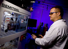
An equipment grant from Semitool Inc. has afforded a University of Houston researcher a sophisticated machine that could make it possible to apply what has been learned in his lab to control stress levels in the thin films used in everyday sensors and magnetic recording devices.
A leading manufacturer of advanced single wafer electroplating and wafer cleaning equipment, Semitool added a brand new version of their Raider M system to Stanko Brankovic’s laboratory in the Cullen College of Engineering this fall. An assistant professor of electrical and computer engineering, Brankovic said the tool is valued at close to $1 million and stands to greatly expand his lab’s capabilities.
“This really has us rivaling that of what is used in industry in places like Intel, Western Digital and Seagate Technology,” said Brankovic. “At the moment, there is nothing out there better than this. There is no academic place in the United States that has this wafer level electrodeposition capability this tool gives us.”
How stress levels evolve in thin films is still not a well-understood phenomenon. So Brankovic has been trying to decipher the science behind why this happens. To do so, he has used a process called annealing to heat the metal in the films to a predetermined temperature, holding it for a certain time then slowly cooling it to improve the films strength. This is in addition to using small organic molecules during thin film’s electrodeposition—a process where metal is deposited on a conductive surface. In each, he is working to understand exactly how adjusting these variables changes the stress level in the films. Using this data, he had hoped to be able to better control the stress that causes curvature in thin films.
The addition of Raider M system will allow him to take this idea one step further, making it possible for him to apply what he learns in the laboratory scale research to industry by attempting to grow these thin films on a much larger, wafer scale.
“Success controlling this curvature in the films on the wafer level would allow us to cut down on the time it takes to develop these films because you would be able to control the stress for the application the film would be used in,” he said, noting their wide use in semiconductor devices, household appliances and automobile instrument panels. “The ability to do this would put the applications these films are used in out to market faster.”
A fully automated, high-performance machine that is tuned to create six inch wafers, the tool is expected to be up and running within a few weeks.
