When a material known as graphene was first produced inside of a lab in 2004, the science and technology community buzzed with predictions that it would become the “next big thing” for the semiconductor industry. Graphene is essentially a one-atom-thick sheet of carbon which conducts heat and electricity with incredible efficiency, making it a homerun material for the semiconductor and electronic device manufacturing industries.
Graphene can also be treated as a two-dimensional building block to create new structures. A bilayer graphene is created when one graphene is stacked on another layer of graphene. Although the basic property of a single layer graphene is well understood, bilayer, especially twisted bilayer graphene, remains a challenge for the scientific community. This is because it is very difficult to describe the lattice and band structure of a twisted bilayer graphene. Depending on the rotation angle, a bilayer graphene may exhibit a periodic structure and become a superlattice, but for many infinitely large number (mathematically) of other rotation angles, the structure is not periodic, making it hard to be handled by traditional band theory. Nevertheless, an artificial interference can always happen between two periodic structures, creating the so-called Moiré pattern – which can be seen many places in daily life, such as through two mosquito window net meshes.
Now, electrical and computer engineering assistant professor Jiming Bao at the UH Cullen College of Engineering has confirmed the band structure of twisted bilayer graphene using Raman spectroscopy. He published his findings in the journal Nanotechnology. His paper, “Four-fold Raman enhancement of 2D band in twisted bilayer graphene: evidence for a doubly degenerate Dirac band and quantum interference,” was also chosen by the journal to be highlighted on their sister website, nanotechweb.org.
Perhaps one of the most puzzling properties of twisted bilayer graphene is that it is essentially a two-dimensional metallic material, making it interact with light and other materials in unusual and unexpected ways. Electromagnetic wave simulations have shown that graphene has the ability to act as an optical waveguide for surface plasmon, essentially serving as a pathway along which these electromagnetic waves can travel. Bao’s group is currently exploring these peculiar plasmonic properties of graphene under the support by a National Science Foundation CAREER Award.
In this latest research, however, Bao’s group revealed a new peculiar phenomenon arising from the unique band structure of twisted bilayer graphene. The samples were synthesized thanks to help from Bao’s collaborator, electrical and computer engineering professor Steven Pei. His group is among the first ones that introduced chemical vapor deposition into graphene synthesis, and has developed mature recipes for both single and bilayer graphene growth.
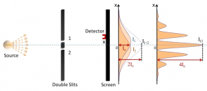
Once the bilayer graphene was synthesized, Bao’s group systematically investigated it using Raman spectroscopy. They adopted the basic concept from the well-known “double-slit” experiment to understand the anomalous Raman behaviors of twisted bilayer graphene. The experiment itself is quite simple, and can be best understood using a basic traffic analogy: in real life, you would expect that two lanes will double the traffic capacity of single lane. But in a quantum world, it can increase four times.
“This is very peculiar. In this case, one plus one equals four,” Bao said of this unexpected finding. “Typically, when you compare Raman intensity between a single layer of graphene and a double layer of graphene, the intensity would double, but in our case it quadrupled.”
The reason for the quadrupled Raman intensity, Bao said, is interference, as observed in Young’s double slit experiment. An increase larger than two has been observed in Raman spectroscopy in the past, but it has never amounted to a quadrupled intensity, as Bao’s group observed. Bao said this finding can be explained by basic quantum mechanics concepts and the unique band structure of the graphene itself.
“In this case, this is classical example or interpretation of quantum mechanics,” Bao said. “We can use this phenomenon to further explore the very interesting product of graphene and further characterize bilayer graphene.” Bao added that with graphene’s enormous appeal to the semiconductor industry, understanding the material and its properties has never been more crucial. “Graphene has applications everywhere – everyone likes graphene. It’s conductive but also transparent, so it can be used for many, many types of electronics and devices – from cell phone screens to photo detectors, and much more.”
Bao conducted much of his work alongside electrical and computer engineering Ph.D. student Yanan Wang, who said she has spent the past two years working with Bao to study the characteristics of graphene. Wang noted that Raman enhancement can be seen from data in previously published papers, but the phenomenon was never reported and used to determine the underlying band structure of graphene itself.
“Actually, this enhanced Raman intensity show up in earlier work by other groups, but they didn’t pay much attention to it, so we got an opportunity to investigate it systematically, related this enhancement to rotation angles and used the quantum interference phenomenon to explain our observation,” Wang said, adding that understanding the underlying characteristics of graphene is extremely important for the electronics industry which wishes to utilize the material for devices. “We need to deeply understand the underlying structure of graphene if we are going to use this material for device packaging. This is fundamental work that allows us to understand its basic properties.”
Both Bao and Wang noted that this research serves as a jumping off point for many more projects seeking to characterize and understand graphene as well as its many potential applications within the electronics and semiconductor industries. For instance, Wang noted that they could now focus on lining up the two layers of graphene slightly differently to try to manipulate the types of interference they observed. “Because we now know band structure of graphene from this Raman result, we could now play around with the position of the two graphene layers and try to use different rotation angles to generate different interference intensities.” Bao noted such a finding could be exploited in the electronics industry for a number of different purposes. “This could allow us to develop photodetectors, such as those found in your cell phone, that are more sensitive to light, or could be used to increase the efficient absorption of solar radiation or to increase the efficiency in converting solar energy to electricity,” Bao said.